Product
NEMST-Matrix2008 series
Atmospheric Plasma Cleaner_Matri
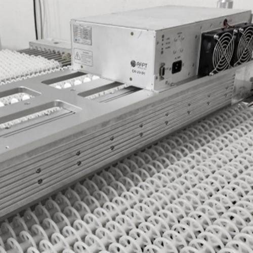
Atmospheric Plasma Cleaner_MatriFeaturing Design
- Dielectric Barrier Discharge (DBD) Plasma Electrodes
- Design With High Plasma Density
- In-direct/Remote Plasma Design with Single Electrode (Water Cooling)
- Using N2 for Reaction Gas
- Electrode width can be designed based on customers' requirements
- Electrodes can be expanded with higher treatment speed
- Gap between Electrode and Substrate is about 2 mm
- Can be Sheet by Sheet or Reel-to-Reel treatment
- Can be standalone machine or module integrated with in-line mechanism
Atmospheric Plasma Cleaner_MatriPerformances
- Single Side Treatment.
- Reaction Gases: N2
- Gap Between Electrode and Substrate: < 2 mm in general. Plasma Effective Width: 100 mm ~ 2000 mm. (Can be larger based on customers' requirements)
- Treatment Speed: 0.5 ~ 5 m / min in general (Can be changed based on customers' requirements)
- In-direct/Remote Plasma Design with no ESD
- Suitable for various materials with sheet or film forms
- High Plasma Treatment Stability and Uniformity
Atmospheric Plasma Cleaner_MatriApplications/Solutions
- Semiconductor & Substrate Technologies: Semiconductors, Wafer surface cleaning, IC Substrates
- Display Process Technologies: FPD, LCD, TP, OLED front-end and back-end glass or film substrate cleaning, ITO Lead cleaning in LCM (pre-treatment for COG/COF)
- Glass Substrate & Modification: Cleaning processes in Cell/Array/LCM stages, surface cleaning and modification of bare/ITO glass substrates (e.g., hydrophilicity improvement)
- General Materials & Film Applications: Surface cleaning for various electronic or non-electronic components (metallic or non-metallic such as PI, PET, PE, plastics, etc.), thin film growth applications